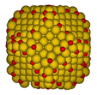
I am simulating low energy electron diffraction (LEED) from a polyfaceted sample. Usually it's a single, well-defined flat crystalline surface.
Since low energy electrons (below a few hundred eV) only penetrate a few monolayers, the allowed diffraction spots are governed by the 2D lattice of the surface rather than the 3D bulk.
For example, I needed to generate the hexagonal lattice vectors for the four distinct (111) planes of a fcc crystal structure. I've done it brute force by doing 3D rotations while imagining the geometry, but I would like to know if there is a formalism that I can use to do it the "right way" such that can be sure the results are correct and can cite the method in a publication.
I'd also like to extend it to the surfaces of (110) and (100) facets.
From the original question post about (111) only:
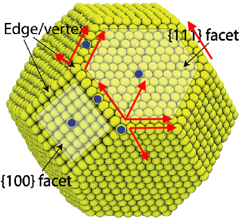
If we slice the corners off of an fcc cube, the exposed (111) surfaces have hexagonal symmetry and can be described by two lattice vectors (with 3 components each) with $\gamma$=60°.
Opposite corners present identical surfaces, so there will be four unique planes, and if we start with one plane, call it "top" (cube sitting on one corner) then each of the other three will share one hexagonal lattice vector with the first plane.
I've drawn them below five atoms long for better visibility.
Question: Is there a straightforward formalism I can both use to get these four sets of two hexagonal lattice vectors, and also cite as a reliable source for it?
Of course if it's "trivially obvious" to everyone else besides me, then perhaps a straightforward explanation or short derivation is all I need.
I think that all eight of the resulting vectors will be in directions with index triplets that contain (-1, 0, 1) in various arrangements with a factor of $a/\sqrt{2}$ in front.
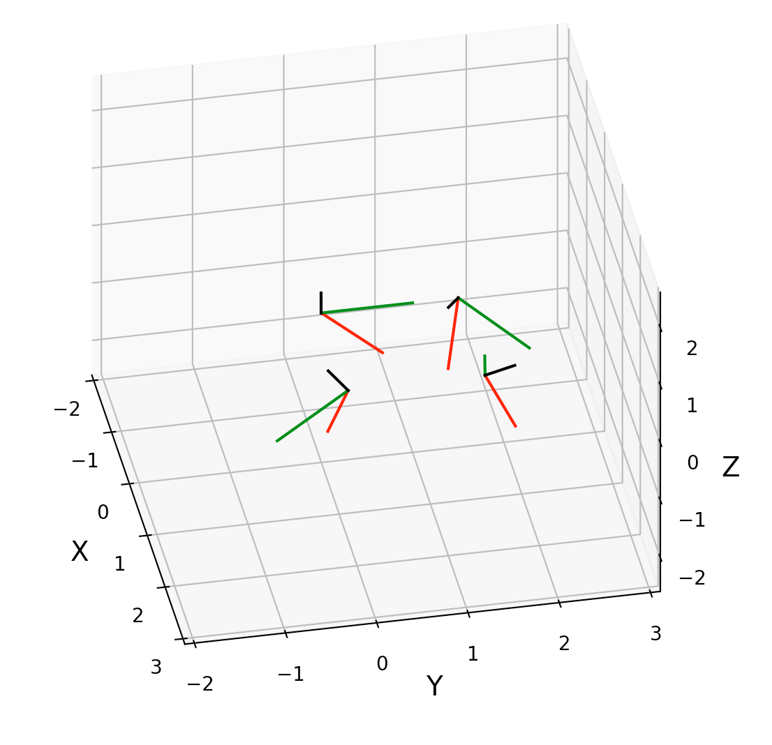
I've made some ad hoc progress, four sets of red/green unit vectors (positioned arbitrarily), the black lines are surface normals. But I am sure there's a simpler, straightforward mathematical way that I've missed.


